Olzhas S. Tazabekov

RF/Analog Integrated Circuit and CMOS-MEMS Designer

with an extensive knowledge of designing RF/analog circuits, MEMS-based resonators and microwave components, comprehensive knowledge of digital integrated circuits and RF communication systems. Well versed in communicating, presenting and interpreting technical information.

Currently is a Senior RF Design Engineer at Broadcom Limited

Carreer Goals: Hands on experience in designing, testing, and analyzing RF modules and components based on both, conventional microwave technologies and MEMS-based resonators. Looking for an engineering position as a part of a professional ambitious and creative team.

My current research includes micro-electro-mechanical systems (MEMS) for RF applications and smart sensors, which incorporate both silicon integrated circuits and micromechanical structures, as well as micro/nanomachining processes and all those cool small things, which can move, sense, be awesome and make our World better.

Résumé

Résumé

Skills

Analog/Mixed Signal Design

  • Semi/full custom transistor level design of various types of analog blocks, behavioral modeling of circuits, layout design and floor planning, DRC and LVS analysis, FEM electromagnetic analysis, PVT/Monte Carlo verifications, experience with industrial CMOS process (0.35um, 0.18um, 40nm, 28nm),
  • System level design and analysis, behavioural modeling using higher levels of abstarctions, specifications and summery of work definition,
  • Solid understanding of low power design techniques, analog/digital design, microwave engineering, solid-state and electromagnetic physics, mechanics,
  • Hands-on experience with lab characterization equipment, e.g. network analyzers, lock-in amplifiers, oscilloscopes, signal generators;
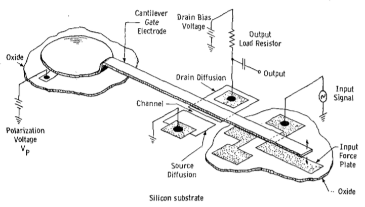
  • Micro-Electro-Mechanical Systems for RF and Sensors

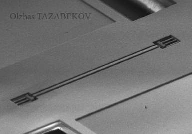
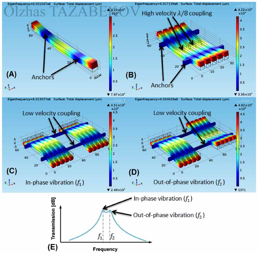
  • MEMS design (electrostatically/electrothermally driven actuators and resonators), 
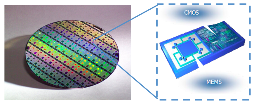
MEMS layout design (optimization for manufacturing and CMOS compatibility), analytical, finite element and behavioral system level modelling,
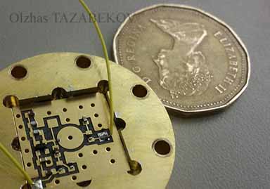
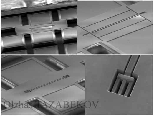
  • Hands-on experience with post-CMOS MEMS fabrication in a cleanroom and fabrication/characterization equipment (reactive ion etching machine, electron and optical microscopes, doppler laser vibrometer);
  • RF Engineering

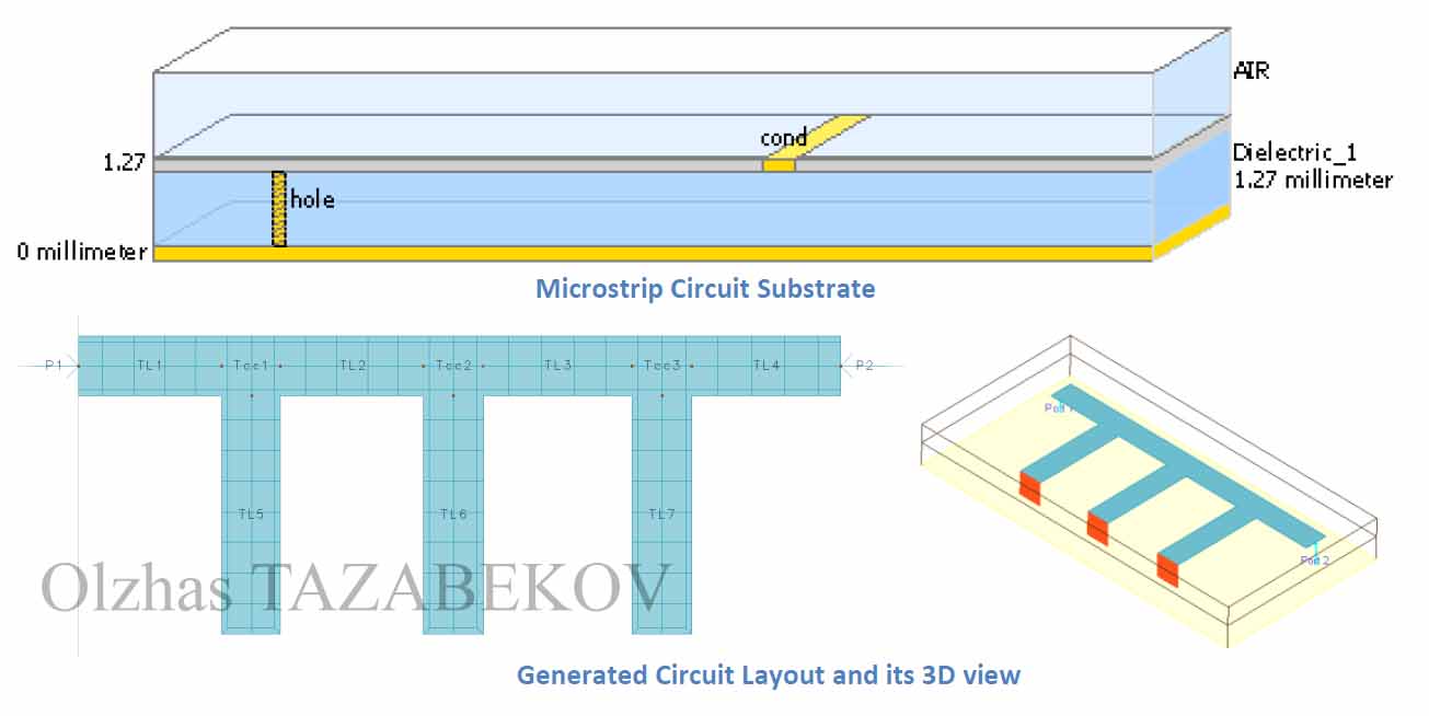
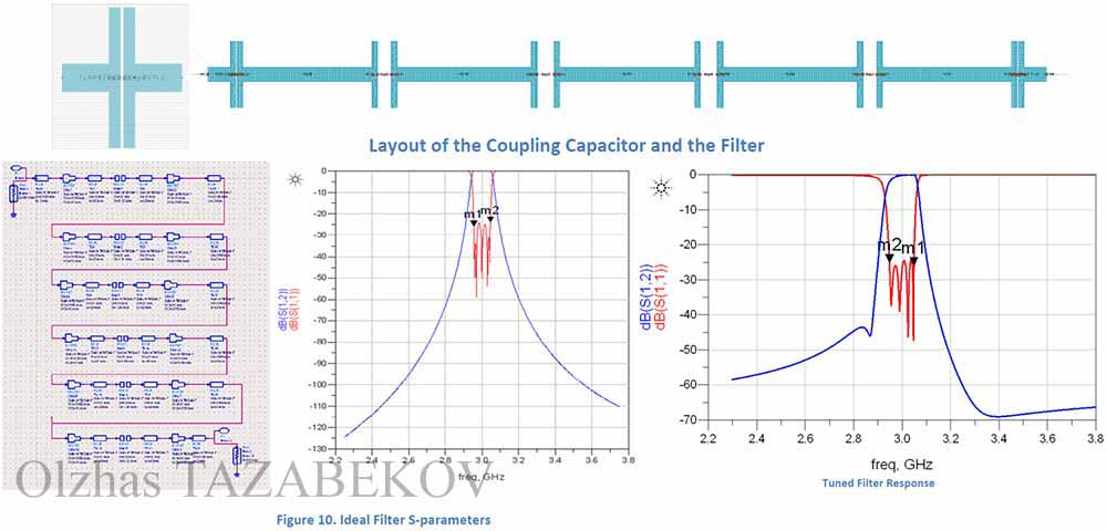
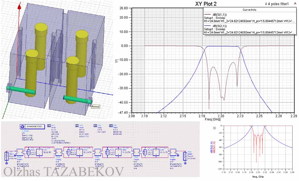
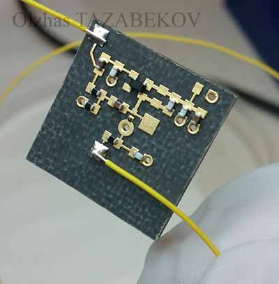
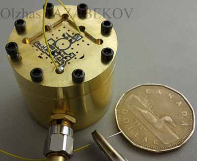
  • RF circuits and passive component desing (e.g. planar microstrip and cavity resonators and filters), EM and circuit simulation, advanced filter design techniques (space mapping, recursuive extraction), solid understanding of microwave theory;
  • Scientific Computing

  • Computational programming and behaviora modelling with Python, Matlab and Mathematica,
  • Solid understanding of object oriented programming, data processing and visualization,
  • Hands-on experience with unix-based operating systems and scripting;
  • Software

  • IC/RF EDA Tools: Cadence IC Design suite, Synopsis IC Design suite, Agilent ADS, Xyce, NGspice,
  • FEM EDA Tools: ANSYS HFSS, Agilent Momentum, COMSOL, Coventor,
  • Numerical Computing Software: Mathematica, Matlab/Simulink, Mathcad,
  • PCB EDA Tools: Eagle, Altium Designer,
  • Programming Languages: Python, VHDL, C++, Pascal, Java, HTML;
  • Areas of Expertise

    CMOS-MEMS for Sensors and Communciations

    Why RF Micro-Electro-Mechanical Systems (RF MEMS) ?

    High frequency mechanical vibrating devices are still widely used in consumer electronics for frequency generation and filtering aplications (e.g. SAW filters and quartz crystals). Compared to active or passive IC elements (e.g. transistors, on-chip capacitors and inductors), mechanical resonators provide higher Quality factors, better linearity and lower power consumption, which is well suited for low-loss on-chip filtering solutions. Continuous size reduction and a possibility of integration with commercially available CMOS IC fabrication process makes RF MEMS technology quite promising for further micro miniaturization of electronics systems.

    Very first MEMS: Resonating gold MOS gate from the 60's [H.C. Nathanson et al. "The resonant gate transistor",IEEE Trans.Electron Devices,vol. , vol. EDED-14, pp. 117–133, 1967.]

    Why CMOS-MEMS?

    CMOS MEMS and Analog IC integrated on a single silicon die

    CMOS-MEMS Design Flow

    The conventional MEMS design flow consists of several steps: design using analytical and FEM methods, layout drawing, post-processing or fabrication and, finally, testing and characterization.

    There are many analytical models built for different types of mechanical resonators (e.g. CC beams, FF beams, disk resonators, lamé resonators, etc.) to predict the critical operational parameters such as resonant frequency, mode shape, maximum deflection, etc. Those are usually used to build initial designs of the MEMS devices that would satisfy the required specs.

    However, analytical models are subjected to many simplifications. That is when FEM methods come to help allowing to refine the initial rough designs to better meet the specifications and obtain the operational parameters with higher precision. FEM methods are also irreplaceable when it comes to analyzing complex structures with no luxury of making simplifications.

    When the overall dimensions of the mechanical structures are finalized one needs to create a layout of the MEMS devices. The layouts are then used to make lithography masks (in case of full in-house fabrications) or passed to the commercial foundry (in case of CMOS post-processing).

    FEM Simulations of Coupled MEMS Resonators Implementing Band-Pass Filter

    SEM pictures of MEMS mechanical resonators

    Quality of the MEMS fabrication or CMOS post-processing might be checked under a Scanning Electron Microscope (SEM), Atomic Force Microscope (AFM) or 3D profilometer.

    To make sure that the fabricated MEMS resonator actually moves and its mechanical vibrating properties such as resonance frequency, mode shape and the maximum deflection are the ones that were desired one may need to use a Laser Doppler Vibrometer.

    Finally, electrical characterization is usually done using network analyzers, signal generators and oscilloscopes.

    Areas of Expertise

    RF Engineering for Communication Systems

    Passive Microwave Component Design and EM Simulations

    Including design of passive planar filters (e.g. microstrip, stripline filters), 3D filter design (e.g. cavity, dielectric filters), etc.

    Microstrip is a type of electrical transmission line which can be fabricated using printed circuit board (PCB) technology, and used to convey microwave signals. It consists of a conducting strip separated from a ground plane by a dielectric layer known as substrate. Microwave components such as antennas, couplers, filters, power deviders, etc. can be formed using microstrip. The entire device exisitng as metallization pattern on the substrate.

    On a smaller scale, microstrip transmission limes are also built into monolithic microwave integrated circuits (MMIC).

    Microstrip circuit

    6-Pole Chebyshev microstrip filter, its equivalent circuit model (ADS) with ideal response and EM simulated response

    4-Pole Chebyshev filter based on microwave cavity resonator with EM simulated response (top), and its equivalent circuit model (ADS) and ideal response

    Microwave resonators and filters can also be constructed from closed sections of waveguides. Because radiation loss from an open-ended waveguide can be significant, waveguide resonators are usually short circuited at both ends, thus forming a closed box, or cavity. A small disc or cube (or other shape) of dielectric material can also be used as a microwave resonator. Dielectric resonators typically use materials with low loss and a high dielectric constant, ensuring that most of the fields will be contained within the dielectric. They are smaller in size, cost and weight when compared to the equivalent metallic cavity, and they can easily be incorporated into microwave integrated circuits and coupled to planar transmission lines.

    RF circuit and PCB design

    PCB with implemented negative resistance circuit

    Microwave resonator and the loonie ;)

    Back to Areas of Expertise

    Analog and Digital Circuit Design

    ...under construction

    Back to Areas of Expertise

    Contacts

    Yes, let's get in touch!

    Email:

    Olzhas.Tazabekov(at)gmail(dot)com